



You are currently viewing a placeholder content from Default. To access the actual content, click the button below. Please note that doing so will share data with third-party providers.
More InformationHigh-energy ion implantation and irradiation services
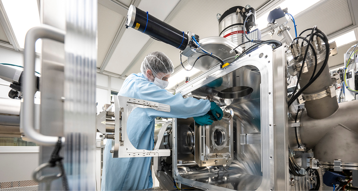
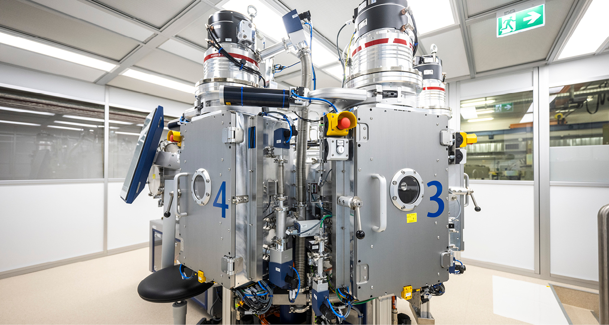
HZDR Innovation GmbH has provided high-energy ion implantation, ion irradiation, and electron irradiation services since 2011. We perform ion implantation and ion irradiation processes to defined specifications for semiconductors, power semiconductors, optical and optoelectronic components, engineering materials, semi standard wafers, wafers and samples non-standard geometries.
Our focus is on reliable processing to customer specifications: clearly agreed process parameters, documented order execution, confidential sample handling, and many years of experience working with customers in Germany and internationally.
Technical capabilities
| Parameter | Description |
|---|---|
| MeV H/He irradiation | H ions up to approximately 8 MeV and He ions up to approximately 14 MeV, depending on the specific process requirements |
| MeV ion implantation | e.g., B, P, As, C, N, and other ion species, subject to technical feasibility review |
| Materials and substrates | Si, SiC, Ge, GaAs, GaN |
| Standard ion implantation | 30 keV to 500 keV |
| Wafer sizes | 2″, 3″, 100 mm, 125 mm, 150 mm and 200 mm |
| Laboratory samples and non-standard geometries | Subject to technical feasibility review |
| Locations | Dresden (DE) and Trnava (SK), each with two MeV irradiation lines |
| Electron irradiation | 10 MeV, through qualified partners |
| Order and process terms and conditions | NDA, product traceability, segregated storage and processing, and an order summary including process parameters |
Typical applications
MeV ion implantation
- Targeted defect engineering in power semiconductors for carrier lifetime control
- Formation of deep dopant profiles
Standard ion implantation (30 keV to 500 keV)
- Doping implantation
- Material modification
- Implantation processes for sensor and MEMS applications
MeV electron irradiation
- Targeted defect engineering for power semiconductors to control the lifetime of charge carriers
FREQUENTLY ASKED QUESTIONS (FAQ)
What ion implantation services does HZDR Innovation GmbH offer?
Our services range from standard ion implantation at 30 keV to 500 keV to high-energy MeV ion implantation, including H/He ion irradiation. We process wafers, laboratory samples, and non-standard geometries using a wide range of ion species. We tailor the process parameters to your specific application.
Are you ISO 9001 certified?
HZDR Innovation GmbH has been ISO 9001 certified since 2015. The scope of certification is: “Execution of production orders in the Ion Technology business segment.” HZDR Innovation GmbH is certified by TÜV NORD. The certificate is available as a PDF.
Can projects be carried out under a non-disclosure agreement (NDA)?
Confidentiality is our top priority. Upon request, we can work under a non-disclosure agreement (NDA) and maintain strict confidentiality regarding your process parameters, samples, project data, and technical know-how.
Do you have experience working with international clients?
We have many years of experience working with customers in the EU as well as in China, other Asian markets, the United States, and other non-EU countries. We communicate with our customers in both German and English.
Can you assist with exporting and importing?
We have extensive experience with import/export procedures and inward processing for a wide range of component types. The specific procedures depend on the sample material, destination country, shipping route, and applicable regulatory requirements.
Ready to implant?
Whether you need a standard implant,
a high-energy irradiation process,
or a custom solution –
talk to us about your application.
Dr. Roman Böttger
Chief Operating Officer
Tel.: +49 351 260 2873
Or send an email
to our sales team: