




Wir freuen uns auf die Zusammenarbeit und beraten Sie gern.

Local lifetime adjustment for power devices using MeV H and He ions

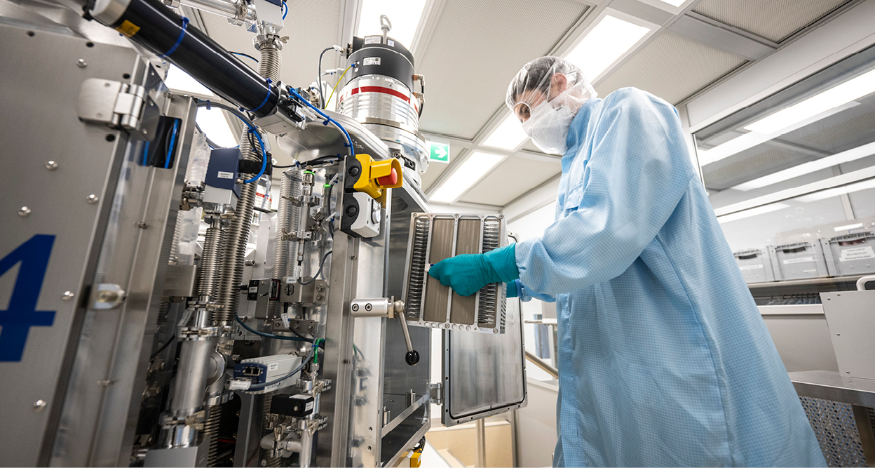
We support semiconductor manufacturers, R&D teams, and process engineers in carrying out defined H/He irradiation runs for defect and lifetime profiling in IGBTs, fast-recovery diodes, PiN diodes, thyristors, and SiC test structures.

 
Why MeV H and He ions? H and He ions in the MeV energy range enable defect profiles at depths that cannot be reached with conventional keV implantation. This allows recombination centers to be selectively introduced into electrically active regions of power semiconductor devices. Particularly in bipolar silicon devices such as IGBTs, PiN diodes, fast-recovery diodes, and thyristors, this approach can be used to investigate and optimize the trade-off between conduction losses, switching losses, leakage current, and device robustness according to specific customer requirements.

HZDR Innovation energy-filtered ion implantation

Which devices are particularly relevant for MeV H/He irradiation?

DeviceRelevance for MeV H/HePotential Benefit
Si-IGBTsVery highInvestigate and optimize the trade-off between tail current, Eoff, and VCE(sat) according to customer requirements
Fast-Recovery-Diodes/FRDVery highTargeted Examination of Qrr, trr, Softness, and VF
Si-PiN-DiodesVery highLocalized lifetime profiles in thick drift regions
Thyristoren/GTO/IGCT-related structuresHighInvestigation of turn-off behavior, recovery, leakage current, and blocking characteristics
HV-Diodes/Press-Pack-DiodesHighDeep defect profiles for high-voltage structures
SiC-PiN/SiC ReliabilityMedium to highDefect physics, carrier-lifetime mapping, and bipolar degradation
SiC-MOSFET Body DiodesSelectiveReliability and body-diode stress studies
GaN-HEMTsLow for conventional lifetime controlPrimarily trap, radiation, or reliability studies
HZDR Innovation Ion irradiation for power semiconductors

Do you have similar questions?

Talk to us – together, we will develop the right solution for your application.

  • Is your fast-recovery diode fast, but switching too abruptly?
  • Are Qrr or trr limiting your next product generation?
  • Does your IGBT exhibit excessive tail current or Eoff?
  • Have you reached the limits of the VF/Qrr trade-off with existing lifetime-control processes?
  • Do you need a localized depth profile instead of homogeneous defect generation?
  • Are you comparing electron-, proton-, helium-, or diffusion-based metallurgical lifetime-control methods?
  • Are you looking for external MeV irradiation capacity for R&D splits or pre-qualification?
  • Are you investigating SiC body-diode stress, bipolar degradation, or defect profiles?

Proton or helium implantation?

IonTypical Positioning
H/ProtonsVery deep profiles and high penetration depths, suitable for deep drift regions and localized lifetime control
HeStronger localized defect generation and different defect chemistry, suitable for creating robust localized recombination centers
H + He combinationDOE approach to distinguish between range, defect, and customer-specific post-treatment effects

The optimal ion species depends on the material, device thickness, target profile, thermal budget, and electrical performance target. Therefore, such projects are typically carried out using a small, customer-defined split-lot matrix before subsequent transfer to volume production.

HZDR Innovation Ion irradiation for power semiconductors

Use cases

Use CaseChallengeApproach
IGBT Turn-off pptimizationHigh tail current and high EoffLocalized H/He defect profiles in the relevant drift region
Fast-Recovery-Diode Lifetime ControlQrr/trr too high or recovery too abruptTargeted lifetime reduction using deep defect profiles
HV-Thyristor / PiN-Diode Defect ProfilingThick silicon structures require localized, deep profilesMeV H/He irradiation instead of relying solely on conventional near-surface implantation
SiC Reliability DOEBody-diode stress, bipolar degradation, or defect mechanisms are unclearDefined H/He defect profiles in test structures or split wafers

High-energy ion implantation

FREQUENTLY ASKED QUESTIONS (FAQ)

What types of ion irradiation do you offer?

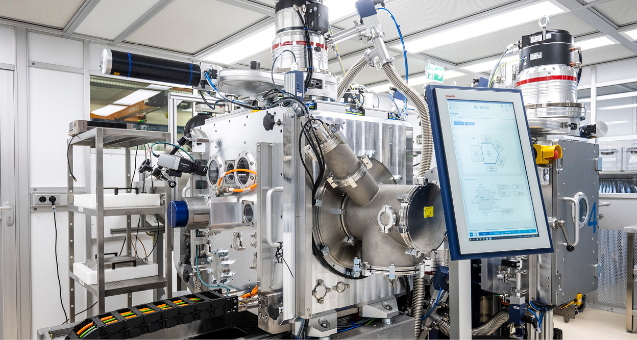
We offer MeV ion irradiation using H and He ions. Typical energy ranges extend up to approximately 8 MeV for H ions and approximately 14 MeV for He ions, depending on the specific process requirements

What are the benefits of H and He ion irradiation for power semiconductors?

High-energy H and He ions can be used to create targeted defect profiles in deeper, electrically active regions of power semiconductor devices. This enables localized modification of carrier lifetime and allows switching behavior to be systematically investigated and optimized. This is particularly relevant for IGBTs, fast-recovery diodes, PiN diodes, and other high-voltage devices.

How long do ion implantation or ion irradiation orders take?

Typical turnaround times are one to two weeks following technical clarification and sample availability. Depending on the specific requirements and capacity, 24-hour services for ion irradiation and ion implantation may also be available.

Why is the maximum allowable process temperature important?

During ion irradiation or ion implantation, the sample may heat up depending on the process parameters and sample configuration. The maximum allowable temperature is therefore a key parameter for assessing technical feasibility.

Do you offer annealing?

Annealing is not part of our service portfolio.

icon_teaser_contact_white

Your contact

Do you have specific ion irradiation requirements or would you like to explore the possibilities for your application? Talk to us – together, we will find the right process for your needs.


Dr. Roman Böttger

Chief Operating Officer

+49 351 260 2873


Or send an email to our sales team:

sales@hzdri.de


Controlled Defects. Enhanced Performance.

Back to the main page about ion implantation