



Wir freuen uns auf die Zusammenarbeit und beraten Sie gern.

High-tech solutions for precise material modification

Electron irradiation enables the precise adjustment of a wide range of physical material properties. We provide targeted process consulting to analyze your specific requirements and identify the optimal approach for your material modification needs.


To help you fully leverage the potential of this technology, our experienced team supports you throughout the process. For applications in semiconductor development, materials research, and radiation qualification, we coordinate 10 MeV electron irradiation through qualified partners and specialized service providers.

 
Upon request, HZDR Innovation GmbH handles the organizational coordination of combined processes and supports the coordination and logistics between the customer, our sites, and our partners in Dresden and Trnava. This provides you with a single point of contact for the entire electron irradiation process.

HZDR Innovation electron irradiation system

Typical applications of 10 MeV electron irradiation

High-energy electrons enable the targeted modification and investigation of materials and electronic devices. 10 MeV electron irradiation is suitable for applications including:


  • Targeted defect generation in semiconductors and other materials
  • Radiation qualification of materials and devices and investigation of radiation-induced changes
  • Comparative studies of different materials, processes, or device variants


The specific irradiation conditions are defined according to the individual application requirements and the technical capabilities of the selected irradiation partner.


What we offer

Benefit from our expertise and a comprehensive range of services tailored to your specific requirements. We combine access to high-performance electron irradiation technology with technical consulting and process support.

  • High-Performance Technology: We provide access to electron irradiation at 10 MeV, enabling targeted material modification even for demanding substrates and offering a high degree of flexibility for a wide range of projects.


  • Efficient Processing & High Throughput: The ability to process suitable wafers in stacks enables very high throughput, making irradiation particularly efficient and cost-effective for larger quantities.


  • Quality & Process Qualification: Our approach is designed to ensure high quality standards throughout the electron irradiation process. We support reproducible processing and consistent irradiation quality.


  • Expert Consulting & Process Development: Our team helps you identify suitable process parameters for your specific material and application. We provide customized solutions beyond standard processes, from R&D and pilot projects through to volume production.

Electron irradiation | Technology & expertise

Detailed information about our electron irradiation services

HZDR Innovation electron irradiation processing

Targeted defect engineering using high-energy electron irradiation

In defect engineering, electron irradiation plays an important role in the targeted generation of defects in materials. High-energy electrons (energy: 10 MeV) interact with lattice atoms, inducing vacancies and interstitial defects. At these high energies, displacement cascades can occur, enabling efficient modification of the material structure at significant depths. This approach can be used to tailor material properties in power semiconductors and other advanced materials.

HZDR Innovation electron irradiation system

Electron irradiation system | Design and operation

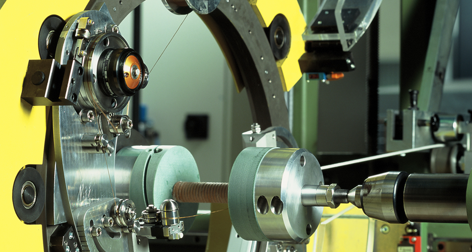
The basic setup of an electron irradiation system consists of three key components: an accelerator, a beam scanning system, and a linear transport system for precise substrate handling. Together, these components provide the basis for controlled and reproducible irradiation processes.

 
The materials to be irradiated are transported at a defined speed through the line-scanned electron beam. The combination of the selected beam current and transport speed determines the applied electron dose. The beam energy is fixed at a monoenergetic 10 MeV. If required, the effective energy can be reduced using scattering plates, although this results in a broader energy distribution. This setup therefore provides both precision and flexibility for a wide range of application requirements.

HZDR Innovation electron irradiation subtrate handling

Substrate handling and material modification

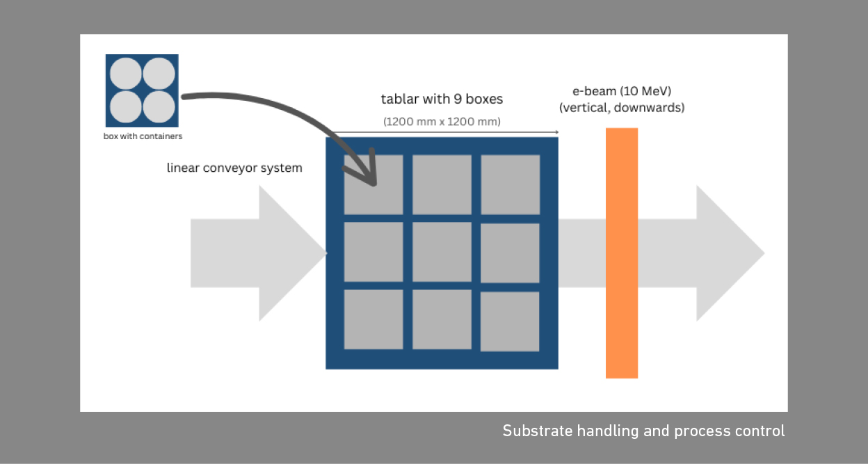
Substrate handling is designed for efficient electron irradiation. Materials such as silicon wafers are stacked in dedicated holders and subsequently placed in irradiation boxes. Depending on the wafer size, several stacks can be accommodated in a single box. Due to their high energy and penetration depth, the electrons can penetrate the entire substrate stack and irradiate the individual layers. This enables high throughput while providing consistent irradiation throughout the stack, supporting efficient and reliable material modification.

HZDR Innovation electron irradiation process control

Efficient substrate handling and process control

he system’s linear transport system is designed to maximize throughput. Multiple irradiation boxes can be placed on a single tray, which then passes beneath the scanned electron beam at a precisely controlled speed. The combination of transport speed, resulting exposure time, and electron beam current determines the required electron dose applied to the material.

 
For processes requiring higher doses, the substrates can pass through the electron beam multiple times to achieve the desired cumulative dose. To improve irradiation uniformity, substrates can also be processed from both sides in individual dose steps. This flexible approach supports uniform and reproducible material modification.

High-energy ion implantation
HZDR Innovation contact High-energy ion implantation

FREQUENTLY ASKED QUESTIONS (FAQ)

Do you offer 10 MeV electron irradiation?

10 MeV electron irradiation is provided through qualified partners and service providers. We can handle the technical and logistical coordination on your behalf. The typical turnaround time is approximately 7 days.

What irradiation parameters are used for electron irradiation?

A fixed monoenergetic energy of 10 MeV is used. Since the required dose strongly depends on your specific material and application, we define the appropriate parameters as part of your individual quotation. This ensures that the irradiation service is tailored to your specific requirements.

Which substrates and materials can be irradiated with electrons?

10 MeV electron irradiation is suitable for a wide range of materials and components, particularly semiconductor substrates and wafers. Due to the high penetration depth, suitable substrates can also be processed in stacks. We assess the suitability of your material, substrate size, and required geometry individually based on your specific requirements.

Do you offer active cooling during 10 MeV electron irradiation?

The substrates are not actively cooled during irradiation. Instead, the total electron dose is divided into smaller increments to ensure that the specified maximum temperature (e.g. 70 °C) is not exceeded. Cooling intervals between individual dose steps help prevent cumulative heating of the wafers.

What additional services do you offer for electron irradiation?

For urgent orders, we offer an accelerated processing option (Rush Service).
We also provide process consulting to help define suitable doses and process parameters for solutions tailored to your specific requirements.

Your contact

Do you have specific electron irradiation requirements
or would you like to explore the possibilities for your application?
Talk to us – together, we will find the right process for your needs.


Dr. Roman Böttger

Chief Operating Officer

+49 351 260 2873


Or send an email to our sales team:

sales@hzdri.de


Controlled Energy. Tailored Properties.

Back to the main page about ion implantation